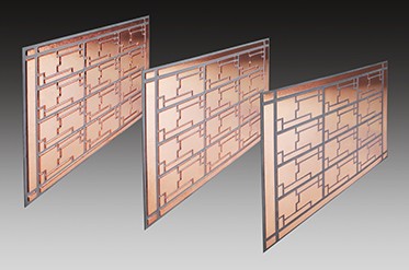
Ceramic Insulating Heat Dissipation Substrates (Pattern Circuit Substrates)
If you have any inquiries, please contact us.
- Tokyo+81-3-3457-4874
Open 9:00am-5:00pm (business days)
Contact UsSilicon Nitride Ceramics: Insulating Circuit Substrates
An insulated circuit board with a copper circuit formed by active metal brazing method on silicon nitride ceramics that have both heat dissipation and strength. We name it "AMC substrate" by active metal brazed copper.
The body of the substrate is made from strong ceramic material and the copper circuit can be between 0.1mm and 0.8mm thick.
Silicon nitride's heat dissipation property makes it a key material for making more compact power modules with higher output. It also has an outstanding heat resistance cycle, resulting in a long life and high reliability in substrates.
This makes it well suited to a wide range of structures in power modules, such as ultrasonic joining of copper electrode terminals, elimination of copper bases and drilled holes for screws.
Features
- Silicon nitride ceramics that have both heat dissipation and strength
- Enables use of thick copper circuits
- Outstanding heat resistance cycle
Product Specifications
Standard Design
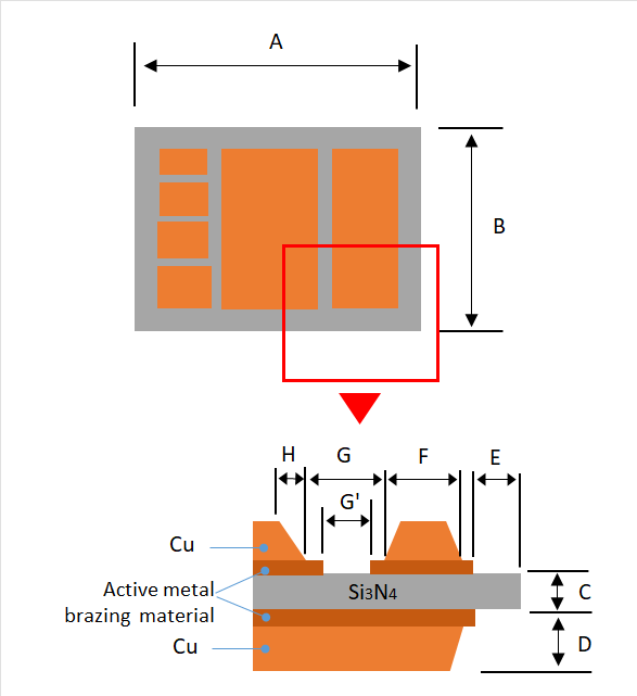
| Ceramics | Type of ceramics:Silicon nitride(Si3N4)。Thermal conductivity 90W/mK(JIS R1611) | ||
| [C]Ceramic thickness(mm) | 0.25 | 0.32 | 0.635 |
|---|---|---|---|
| Tolerance(mm) | ±0.05 | ||
| [A,B]Ceramic dimention(mm) | Maximum effective area_90×110 ※For ceramics with a thickness of 0.25mm/0.32mm, we may be able to make sizes up to 125mm x 165mm, so please contact us for details. |
Tolerance(mm) | ±0.15 | ±0.20 |
| Electrode material | Cu | ||||||||||
| [D]Cu thickness(mm) | 0.10 | 0.15 | 0.20 | 0.25 | 0.30 | 0.40 | 0.50 | 0.60 | 0.70 | 0.80 | |
|---|---|---|---|---|---|---|---|---|---|---|---|
| [E]Insulation distance(mm) | min.0.5 | min.0.7 | min.1.0 | ||||||||
| [F]Pattern dimention(mm) ※The bonding surface on the ceramic side is used as the reference. ※Please contact us if you have any specifications for the top side dimensions of the copper pattern. |
min.0.4 | min.0.5 | min.0.7 | min.1.0 | |||||||
| [G]Insulation distance(mm) ※The insulation distance between patterns[G'] must satisfy the minimum dimensional distance. |
min.0.4 | min.0.5 | min.0.6 | min.1.0 | min.1.2 | ||||||
| Pattern Tolerance(mm) | ±0.2 | ±0.3 | ±0.4 | ±0.5 | |||||||
| [H]Taper dimention(mm) | ≦0.5D(less than 1/2 of the Cu) | ||||||||||
| Warp(mm) | 0.2/50 Under | ||||||||||
| Surface roughness(JIS B 0601:2001) | Rz≦15,(Ra≦6) | ||||||||||
| Peel Strength(JIS C 6481:1996) | ≧9.8kN/m | ||||||||||
| Plating | Electroless plating Ni / NiAu | ||||||||||
| Plating thickness (any measurement point) | Ni:2~6μm / Ni:2~6μm,Au:0.05~0.1μm | ||||||||||
| Solder Resist ※Please contact us if you have a specific solder resist. |
UV curing type / Thermosetting type | ||||||||||
| Solder Resist Thickness | 5~45μm | ||||||||||
*The value of a table is not a guaranteed performance.
*Please contact us for possibility of correponding to designs not covered in above chart.
Joining method of copper circuit
In our AMC (active metal brazed copper) substrates, the copper circuit is joined to the ceramic material with a brazing material in between.
This makes it easy to create fine patterns, and produces power module substrates with outstanding heat resistance and cost effectiveness.
* Contact us for details on aluminum nitride insulating circuit substrates
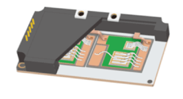
Examples of uses
- Power modules (inverters/converters)
Benefits for customers
- Higher output
- Smaller size
- Low loss
- Long life/greater reliability